Difference between revisions of "SLL"
m (Protected "SLL" ([edit=autoconfirmed] (indefinite) [move=autoconfirmed] (indefinite))) |
|||
| (3 intermediate revisions by 2 users not shown) | |||
| Line 9: | Line 9: | ||
<tr><td>Output Flags</td><td>[[Sign Flag]], [[Zero Flag]]</td></tr> | <tr><td>Output Flags</td><td>[[Sign Flag]], [[Zero Flag]]</td></tr> | ||
</table><br/> | </table><br/> | ||
| − | The Shift Logical Left ( | + | The Shift Logical Left (SLL) instruction shifts the bits in the specified register by either one (1) or two (2) bits to the left, stores the result back to the specified register, and sets or clears the [[Sign Flag]] and [[Zero Flag]] according to the new value in the register. The leftmost one or two bits are discarded and the rightmost one or two bits are set to zero(0). The number of clock cycles used depends on the number of shifts specified. One shift will use 6 clock cycles and two shifts will use 8 clock cycles.<br/><br/> |
| + | |||
| + | [[Image:Sll_diagram.png]] | ||
| + | |||
| + | |||
| + | The opcode format is as follows.<br/><br/> | ||
0000:0000:0100:1srr<br/> | 0000:0000:0100:1srr<br/> | ||
| Line 19: | Line 24: | ||
rr indicates the target register | rr indicates the target register | ||
such that: | such that: | ||
| − | + | rr == 00 indicates register R0 | |
| − | + | rr == 01 indicates register R1 | |
| − | + | rr == 10 indicates register R2 | |
| − | + | rr == 11 indicates register R3 | |
Latest revision as of 09:12, 4 December 2010
| Instruction Name | Shift Logical Left |
| Mnemonic | SLL |
| CP1610 Clock Cycles | 6 or 8 |
| Interruptible | No |
| Opcode Range | $0048-$004F |
| Input Flags | None |
| Output Flags | Sign Flag, Zero Flag |
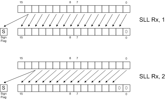
The Shift Logical Left (SLL) instruction shifts the bits in the specified register by either one (1) or two (2) bits to the left, stores the result back to the specified register, and sets or clears the Sign Flag and Zero Flag according to the new value in the register. The leftmost one or two bits are discarded and the rightmost one or two bits are set to zero(0). The number of clock cycles used depends on the number of shifts specified. One shift will use 6 clock cycles and two shifts will use 8 clock cycles.
The opcode format is as follows.
   0000:0000:0100:1srr

   where:
       s   indicates the number of places to shift
           such that:
               s == 0   indicates to shift once
               s == 1   indicates to shift twice

       rr  indicates the target register
           such that:
               rr == 00   indicates register R0
               rr == 01   indicates register R1
               rr == 10   indicates register R2
               rr == 11   indicates register R3
